I’ve been sour on education lately. Given my entry into the field, I felt it prudent to explain myself.
In general, I’ve been well served by my own education. I went to a great public school system where I grew up and I went to Case Western Reserve University (CWRU) for my undergraduate degree in EE (I have neither a Master’s nor PhD). I had decent grades (solid B+ student throughout my tenure) and I had a good experience with my classmates. So what gives? Why do I complain about education?
One reason is that the real value that came out of CWRU was the co-op program. It was run well and it was my two jobs as a student (taking 7 months off from school at a time) that truly taught me about the nature of electronics. In fact, the hands on stuff is where it all came together (as it often does). And then, looking back towards the theoretical teaching that I learned I started scratching my head as to why it was taught in such a way.
Because it’s always been taught that way.
That’s about the best I can come up with. Sure the math matters (really, it does). And learning about the equations behind resistor dividers or op amp circuits does a lot for students’ eventual need to solve problems. But why were we learning it? What were these mystical devices? Why did I only see them drawn as symbols on a page and not hold one in my hand. Most importantly, why didn’t anyone seem to care about that fact as they showed me that V=IR?
The missing piece was that the University setting started ramping (for electronics) around the time that long-time hobbyists entered the school. Many students entering the electronics programs in the 50s and 60s were at home tinkering with radios and kits while they were younger, so the program teaching the math behind these components fit into the mindset of the incoming students. Some students still enter with this background, of course, but even in the event that a student has been working on hobby electronics for 15 years before entering University, the focus will not be on the practical. Why?
I’ve heard other reasons, that the practical stuff is too specific. You can’t go and teach someone how to use a specific piece of software or a specific bench tool, because the material would be quickly dated (obviously they had never glanced at the tools being used by academia, as those are often ancient in all but the highest research areas). Instead the focus once again moves to the math and the equations that govern ideal behavior. An important concept, but not nearly as useful when used in isolation.
My opinion is that the system feeds back upon itself; students are expected to become PhDs who are then expected to teach students. Coursework is constructed to fit that end goal. The ones who survive are the ones who did the best at mastering the theoretical and the ideal. No room is left for the practical and even if there were, the ones teaching are not well versed in it (with the possible exception of the ones that are hands on in research labs). However, in an engineering school, very few are going to become professors (tenure track positions continue to decline while the number of PhDs continues to grow) and many more are going to enter industry where the practical skills are expected. Schools assume on the job training will take care of the rest (or senior project type courses), while employers continue to cut training budgets and have ridiculous job requirements for entry level positions.
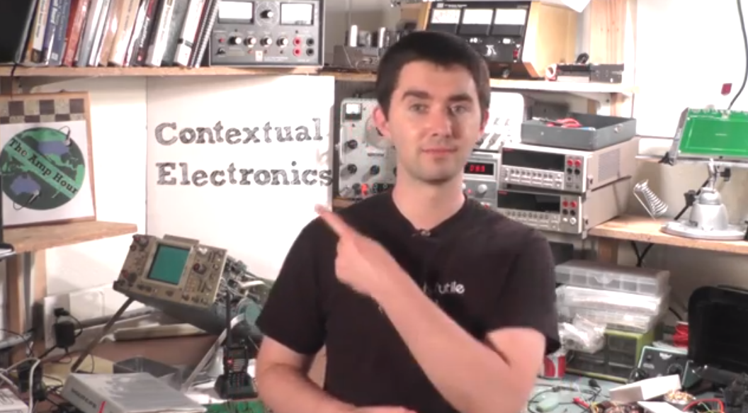
So I decided to build my own thing. I want to give people the context they need to build electronics.
My initial idea for Contextual Electronics was formed out of frustration. Why doesn’t anyone teach this stuff? Schools don’t. Workplaces don’t. Online, very few do (and they’re often scattered across the web, piecemeal). OK, so that looked like there was a need. But what should I teach?
- PCB Design — This was a skill I used often but rarely was taught in any manner. It was more of “figure it out”. I did, but I made some costly mistakes along the way.
- Analog — I had a lot of trouble with signal chain stuff when I left school, regardless of the fact that I took classes in it throughout school. This also was a topic not as widely covered with online resources. Seeing as this has been my main area of employment since then, I thought it worthwhile to share my struggles and how I got past them.
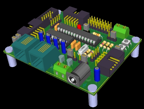
- Tool building — At the suggestion of a friend, I decided to work on something that would be a useful tool on my bench. This allowed me to teach something that has direct applicability, but also something that will be flexible enough to build upon later.
- Supply chain — One of the biggest shocks to the system when leaving school and thinking I knew how design worked (or even in my co-op days) was the “other stuff”. Turns out when you make things, you’re really just piecing together other things…and that means you need to purchase those other things.
- The “putting it all together” — The tough part in any field is associating the theoretical with the practical. Oftentimes, this isn’t perceived to be a separate field of study, but I think it is. If you assume theoretical things will “just work”, you’re going to get burned. If you think practical things will “always work”, you’re going to be iterating without any direction and will also get burned. The method of taking assumptions from the theoretical predictions and using experiments to verify these claims in a real world context (there’s that word again!) is something that needs more focus. In fact, even in this first session of Contextual Electronics, it can use a lot of work.
- The “just do it” mantra — Again, a nebulous topic, but something I wanted to emphasize in the course. Having guidance is nice and will be provided to students. But you need to jump in and make mistakes. So that’s another part of this course, to the point where the finished PCB likely will have some mistakes. Instead, we can call them “learning opportunities”. Session 1B, where we’ll be building and debugging hardware, will be all about this trial-error-analysis cycle.
- Openness — Another misgiving of the academic path is built into the structure of the institution; there are large competitive edges in keeping your work quiet or secret in an age of openness and sharing. So the course will use open tools (KiCad, SPICE), will produce open tools (all products will be licensed as Open Source Hardware) and much–though not all–work will be shared online (progress of the project is shared on GitHub).
I’m not saying that Contextual Electronics is perfect or finished. Just that it’s starting and that it’s an outgrowth of my frustration with the state of electronics education. I hope you consider taking the course. If you do, there’s more info about it here: http://contextualelectronics.com/session-1a-registration-is-now-open/
Thanks to Nick Thompson for the image of Aristotle