Categories
Analog Electronics Learning Renewable Energy

Switching Regulators and Switching Noise

A background

Switching regulator, buck converter, boost converter, SEPIC, flyback, push-pull, buck-boost… do you know what the heck these things are??? Because I sure didn’t when I was getting back into analog electronics. Now thanks to new interest in power efficient electronics, they are starting to come front and center on the electronics stage. Hopefully this article will give you a better understanding of what they are, what they do, where to use them and issues with noise.

OK, so before we get to the real topic of this post, what do switching regulators do?

Switching  regulators allow you to translate one voltage into another. They allow you to take a higher voltage and translate it to a lower voltage or a lower voltage and go to a higher voltage.

“Eureka!” you cry, “Chris has found the solution to all of our energy needs! We just hook a bunch of these switching doo-dads up and we’ll have unlimited power!”

But no, it’s not that easy. Switching regulators go off the fact that you can take a voltage and translate it to a different voltage, however, the power stays the same (in an ideal case). Meaning if you have 5V coming into a circuit and you have a portion of that circuit that needs to operate off of a 15V supply, you can use a boost converter or something similar and crank up the voltage. Say you have 150 mA (at 5V) coming in, when you convert it up to 15 V, you’ll have 50 mA available to whatever needs the 15V power. Notice in this (ideal) case, the power stays the same (750 mW).

It is a similar story when going down  in voltage. However, there are many more options when moving down in voltage: switching regulator, linear regulator or even a passive element (like a resistor or a diode). You use a switching regulator because they regulate the output voltage (unlike the voltage drop across a resistor or a diode) and they don’t waste power like a linear regulator. If you want to go from a 20 V input down to a 5V output, a linear regulator would just “burn” up that 15V in the middle. With a switching regulator, most of the power is conserved (assuming you are running in the optimized voltage ranges…and there are a ton of different models to choose from so you can find the right range).

Finally, real quick, where are these used? Well, the hot new talk of the town has been renewable energy. “I can get 95% efficiency?” you ask, “Why wouldn’t I pay $4 per chip to do that?”. And really, the power efficiency isn’t just the garbage everyone seems to be spewing these days about saving energy for savings sake…it actually can help you make a better product. If you are in a heat sensitive situation, you don’t want to use a linear regulator to get your required voltage. In the above example if you are going from 100 mA at 20V and the output of the linear regulator is 100mA at 5V…that means you are burning 1.5W just regulating your voltages. With a switching regulator you can save a good percentage of that (for battery or “green” devices) and you can reduce the heat in a sensitive application. Plus, if you’re trying to go from a lower voltage to a higher voltage, you’re out of luck with linear regulators.

Switching Noise

Nothing in life is perfect. Switching regulators aren’t 100% efficient, there are limits to how much you can convert voltages (1000v down to 10V usually isn’t possible…or smart) and even in the best cases a switching regulator will introduce noise into a circuit. For the ways I have mostly used switching regulators (supplies for digital circuits), switching noise isn’t that big of a deal. If you are supplying 5V to a piece of flash memory, the part will probably not care if there is 100 mV of noise “on top” of the 5V signal (meaning the actual power supplied would bounce between 4.9V and 5.1V). Same for supplying power to LEDs or other non-analog situations. However, if there are any measurement components in your design or any even slightly sensitive analog portions, you should consider how the switching noise will affect your output.

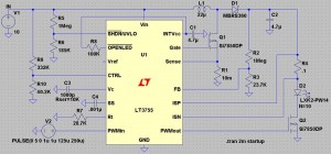
So why does switching noise occur? To answer that we really need to look at a switching regulator to understand what is inside of it. To illustrate, I will be using my version of LTSpice, which is free (awesome!). Also to note, there are lots of great programs out there to help you design this stuff (Webench, for example). Just don’t want to leave any of the vendors out, especially when they give out sampled parts. For this example, we’ll look at the LT3755, which EDN (and me by extension) showcased in an article about creating simple LED lighting for your home.  The application here would be to boost an input of 10V to an output of 40V to light an array of up to 14 1A LEDs.

lt3755

Notice the LEDs (D2 in the diagram) are where the final current and voltage is being delivered. The waveform for the inputs and outputs is below:

lt3755_chart_no_i

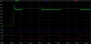
In this graph we see the voltage at the point above R4 (the sense resistor), which is close to what is being delivered to the LEDs. Notice that the voltage starts at roughly 15V and then shoots up to around 40V; the “on” state when the LEDs would be lit settles around 38V. When the red PWM waveform turns off, the voltage bounces up to the exact voltage (40V) the LT3755 is supposed to be outputting because the LEDs are not draining on the output of the circuit. When the PWM goes back on (to 5V), there is noticeable noise on the output voltage. So why is there noise?

lt3755_chart

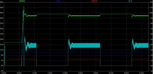
If you look at the circuit diagram above, the second most critical component after the regulator itself is the inductor (L1), just to the upper right of the LT3755. Switchers take advantage of the fact that the voltage across an inductor is equal to the instantaneous current through an inductor times a constant (known as inductance). Pulsing current through the inductor introduces the voltages necessary to step the output voltage up to the desired level. Using negative feedback, the controlling chips can output pulses at varying speeds and shapes to correct for any errors on the output of the circuit (see the image above to see the current going through the inductor in light blue). However, as stated before, nothing is perfect. The bandwidth of the chip (the op-amps and other controlling elements within the chip) are finite, so there cannot be perfect control. This introduces noise on the output of the circuit at the same frequency as the switcher (and some harmonics of that frequency).  In the LT3755, the switching frequency can be anywhere from 100 kHz to 1 MHz.

If you are using this switcher for LEDs in a car…no big deal. And really, with high power applications such as lighting, the noise isn’t much of an issue. However, as switching regulators find their way into more and more products, the noise issue becomes more prevalent, especially smaller products. The trade-off comes in when you start looking at the inductor required for the switching regulator. Some can get quite large and unwieldy, especially for handheld products (see below for an unwieldy example).
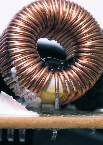
So instead of using a large value (and size and price) inductor, the switching frequency needs to increase. As explained before, voltage is created across an inductor by forcing pulses of current through the inductor. The higher frequency means that there are smaller current pulses, but there are more of them. This allows for smaller and smaller inductors in designs (some are starting to be pulled into the chip packaging!) but brings with it the noise, now at a higher frequency.  If you have a 5V power supply line with 100 mV of noise of top of it (with the noise at around 100 kHz), then it might not be a problem on your circuit board. But when your boss tells you to start using smaller parts so you can fit the design in a handheld form factor and the switching frequency goes up to 1 and 2 MHz, you will start having problems. That innocent 100 mV from before now might couple into other board traces and introduce noise into the rest of your design. If you have any analog signals that are critical to your design, 100 mV of noise can wreak havoc on the output.

Less noise, more answers

Switching noise is something that will be apparent in any design involving a switching regulator. Knowing your system constraints will allow you to best decide which option is best for your specific needs. If you are crunched for space, you will need to be able to handle high frequency switching noise. If you are sensitive to noise, you better buck up for some big, expensive inductors and carefully route your board (in fact, if you’re that sensitive, maybe reconsider switching regulators entirely). If you have access to the resource, the best people to ask are the vendors selling the parts; they know the funny behavior of a part and which “flavor” of regulator to use to best suit your needs. And in the meantime you can play around with the tools they make available online and in software.

Please leave any questions or comments you might have and good luck with your new designs!

Categories
Analog Electronics Digital Electronics Engineering

Circuit Board Design (And How It Has Changed)

Products today mostly use Printed Circuit Boards (or PCBs) to successfully route signals from one component in a circuit to the next. There are multiple layer circuit boards with printed metal “wires” that run between the various elements in a circuit. However, this was not always the case. In the good ol’ days, there were different variations and precursors to the PCB. Some of these included point to point wiring (just soldering a wire between say a resistor and a capacitor), wire wrap boards (think of a point-to-point board on a grid with more wires than you’d know what to do with), acid etched copper on dielectric (think of a 1 layer PCB with very large and rounded signal traces) and many others. These kinds of boards had many many different methods but also had less restrictions than modern designs. In fact,  Paul Rako from EDN recently wrote a great article on prototyping using some of these older methods. He references many techniques of the greats like Bob Pease and Jim Williams and their rapid prototyping techniques. It’s an information rich article and I would highly suggest checking it out. OK, back to the party.

So what has changed when moving from older boards and circuit designs to newer circuit boards?

  1. Speed — There’ s no denying that the boards of today are faster than those of yesteryear. The extremes are apparent in the RF industry which is/was doing well because of the cell phone becoming the hottest platform to develop for (PCs are still around of course but the excitement is in the cell phone industry).  When frequencies get into the GHz range and you’re trying to guide signals instead of wire them, you know that your boards will be finicky. Additionally, the speed increase is not limited to the RF industry as many new designs have at least some component of a clocked digital system on them. Even pushing into the MHz range can be difficult with older board techniques. Wiring point to point is not as viable with high speed signals, especially when you have upwards of 32 wires between two components (a data line).
  2. Size/Type of components – This is another symptom of newer industries. As products go increasingly mobile, parts begin to shrink out of necessity or because the cost of making the older, larger parts becomes prohibitive. As such, the boards have made a large change going from through-hole components (like the capacitors in the picture at the top of this site), to Surface Mount Technology. This has affected the construction of final boards (SMT usually requires machine placement for quick and reliable boards). This also means that the amount of power a board containing only SMT parts can absorb (when the board is considered as one entity) is reduced as the smaller SMT parts cannot handle as much current without blowing up.
  3. Number of connections — I’ve included a picture of wire wrap from the Wikimedia commons site below. Notice anything about it? It’s ridiculous! And I would encourage you to go to the Wikipedia page and look into some of the other types of wire wrapped boards. Now let’s look at a common package today, the Ball Grid Array (BGA). This type of package uses little solderballs on the bottom of the package to adhere to the board. It is glued on at first and when you reflow (heat up to make the solder melt), the balls fall into place on whatever PCB you have produced (assuming you have made the PCB correctly).  BGAs start around 144 pins (maybe 196?) I believe and go to upwards of 1000 pins per part. Can you imagine trying to hook up 1000 wires like below? I don’t think so.
  4. RoHS — Lead is bad for the environment, for your health and for any children who decide to ingest it. In fact, the only people who speak the wonders of lead these days are cranky analog engineers such as myself, trying to solder something (I’m a 6 out of 10 on the cranky scale). Why do we love lead? Because Lead-Tin (Pb-Sn) solder is much easier to work with due to the lower melting temperature and higher thermal capacity.  So as RoHS becomes more widespread, with the Silver-Tin (Ag-Sn) solder that is more difficult to work with, it become another element of board design that must change.

So obviously some stuff has changed. Some is for the better, some not so much. Let’s look at board problems encountered in modern day printed circuit boards in order to see the problems encountered as circuit boards have become more inexpensive and repeatably made:

  1. Capacitance in the board — Printed circuit boards are constructed from a non-conducting material so that signals do not leak from one lead to another. However, in constructing the perfect insulator, they also created a material with a significant (but not huge) dielectric constant. This means if two signals are routed over top of one another (acting like plates), then the sandwich of the signal and the dielectric will act like a capacitor. Not only that, but as you increase the frequency of a signal (with speeds upwards of GHz), the capacitor looks more and more like a shorted wire! This phenomenon is known as “cross-talk” and can affect myriad high-speed or high voltage situations.
  2. Inductance in the leads of a chip — Before the BGAs mentioned in point 3 above, there were packages (usually square) with leads coming out the sides known as Quad Flat Packs (QFPs). The leads coming out of them vary in thickness, but usually get thinner as there are more leads on a chip. As the leads get thinner and longer, the inductance of those leads goes up. We remember that inductors are the “opposite” of capacitors in that they allow low frequency signals to pass and block high frequency signals. In a system that is mostly high frequency signals (think digital), the inductance of the leads can have a serious affect on how well a signal propogates from one element on a circuit board to the next. BGAs have started to reduce this problem, but the cost of dealing with BGAs can be quite prohibitive for smaller operations.
  3. Timing — In a high speed system that requires signals to depart a component at a certain time and arrive at a different component a short (predictable) while later, there are many things that can prevent the signal from arriving undisturbed. We’ve already seen the capacitive and the inductive effects mentioned above, but what about resistance?  Although everything has some amount of resistance, the lines in a board routing one component to the next can have an affect on the overall performance of a circuit. If one of these lines is longer than another than there will be a noticeable difference in the resistance of that line. Most importantly, when comparing the impedance (sum of the resistance and the frequency dependance of the impendance and capacitance) of two different lines going between components (say a processor and a RAM chip), differences can cause the signals to arrive at different times in different conditions. The rise times, the fall times, the over shoot, the under shoot, and the general shape of a signal can all be affected by the characterisitcs of the connection. It is useful to remember that every connection really acts like an RLC filter circuit, the only difference being how much resistance, inductance and capacitance are present and how they will affect the final signal.
  4. Ground/Power Plane — Other advantages a circuit board brings, especially multilayer circuit boards, is the ability to route a plane of power or a grounding plane underneath a portion of a design. If we think of a PCB as a large sandwich, the grounding plane would be like a slice of cheese, running underneath many of the different components of a circuit but not necessarily connected to them. If you design a circuit to have “vias” then an example component on the very top of a circuit board can connect down to the plane and access the power, ground or whatever signal happens to be running underneath there. This technique can be quite useful if you have many different op-amps in a certain area that will require positive and negative power supplies. Or if you have a large connector that requires a majority of pins to be grounded, a grounding plane can be useful to quickly connect many signals to the same net. However, as with any system, there are real-world consequences to deal with; in this case, we have to deal with electrons acting like electrons. With grounding planes, all of the pins on a board that are tied to ground will technically be at ground, however if one pin happens to have a large current going into the ground, then that area might have a slightly higher potential (voltage) than other ares of the grounding plane. This could have some definite effects in sensitive electronic situations and should be considered when designing a new PCB.
  5. Heat/Warping — A major downside to PCBs is the rigidity of the material; worse, when it heats up, it can often warp and become unusable. This could also be a problem in acid etched and wire wrap boards (the warping), but since the connections are often either larger traces or wires, the chances that the warping would break the connection are lower. Worse yet, the example above (dumping current into a ground plane) can create its own heat and warp a board without even being in a heated environment. Thermal budgets become important in any new PCB design and you should be mindful of them. Some SPICE programs even allow you to check out what the heat/power dissipation will be before putting the components on a board.
  6. Low Power — Unfortunately for high power circuit manufacturers, PCBs require extra care when they contain high voltages or high currents. Newer boards are often optimized for power savings, so high power situations are not as much of a priority for the tools that create PCBs. There are often constraints in the layout programs to ensure proper safety requirements, but other steps might be necessary, like separating high power lines from one another so they do not spark or create noise on other lower power lines.

Printed circuit boards allow for reliable products that can quickly be deployed to customers or used in a lab situation to test new circuit configurations. As long as you are mindful of the pitfalls of PCBs listed above, you can create circuit designs that can do just about anything imaginable.  If you have any suggestions on how to create better PCBs or circuits in general, please leave your thoughts in the comments.

Categories
Analog Electronics Digital Electronics Engineering Learning Life Work

How to get a job as a new electrical engineer grad

I was going to call this post “A portrait of an electrical engineer as a young man (or woman)” but decided against it. I’ve got nothing on James Joyce, neither in loquaciousness nor confusing writing.

Anyway, I have been pondering what kind of employee I would hire out of school for an electrical engineering position. There are some basic skill sets that will allow just about any young engineer to succeed if they have these skills (the best situation) or at least appear they will succeed if written on their resume (not the best situation). Either way, let’s look over what a new grad should have on their utility belt before going out into the scary real world.

  1. Conceptual models of passive components — This has been one of the most helpful things I have learned since I have left school…because this kind of thinking is not taught in classrooms (at least it isn’t in the curriculum). The idea is to conceptualize what a component will do, as opposed to what the math is behind a certain component or why the physics of material in a component give it certain properties. Why does this matter? When you’re looking at a 20 page schematic of something you’ve never seen before, you don’t care what kind of dielectric is in a capacitor and how the electric field affects the impedance. Nope, you care about two things: What is the value and how does it affect the system. The first question is easy because it should be written right next to the symbolic notation. The second is different for each type of passive component you might encounter. Let’s look at the common ones
    • Resistors — The  best way I’ve found to think of resistors is like a pipe. The electrons are like water. The resistance is the opposite of how wide the pipe is (if the resistance is higher, the pipe is smaller, letting fewer electrons through in the form of current). Also, the pressure (voltage) it takes to get water (electrons, current) through a pipe (resistor) will depend on the thickness of the pipe (resistance). Well whaddaya know? V=IR!
    • Capacitors — At DC, a capacitor is essentially an open circuit (think a broken wire). If you apply charge long enough (depending on the capacitance), it can consume some of that charge; after it is charged it will once again act like an open circuit. When considering AC (varying) signals, the best way to think about a capacitor is like a variable resistor. The thing controlling how much the capacitor will resist the circuit is the frequency of the signal trying to get through the capacitor. As the frequency of the signal goes up, the resistance (here it is called “impedance”) will go down. So in the extreme case, if the frequency is super high, the capacitor will appear as though it is not there to the signal (and it will “pass right through”). Taking the opposite approach helps explain the DC case. If the signal is varying so slowly that it appears to be constant (DC), then the impedance of the capacitor will be very high (so high it appears to be a broken wire to the signal).
    • Inductors — Inductors have an opposite effect as capacitors and provide some very interesting effects when you combine them in a circuit with capacitors. In their most basic form, inductors are wires that can be formed into myriad shape but are most often seen as spirals. Inductors are “happy” when low frequency signals go through them; this means that the impedance is low at low frequencies (DC) and is high at high frequencies (AC). This makes sense to me because if the signal is going slow enough, it’s really just passing through a wire, albeit a twisty one. An interesting thing about electrons going through a wire is that when they do, they also product tiny magnetic fields around the wire (as explained by Maxwell’s Equations). When a high frequency signal tries to go through the inductor, the magnetic fields are changing very rapidly, something they intrinsically do not want. Instead it “slows” the electrons, or really increases the impedance. This “stops” higher frequency signals from passing through depending on the inductance of the inductor and the frequency of the signal applied. Looking at the how they react to different frequencies, we can see how inductors and capacitors have opposite effects at the extremes.
    • Diodes — I think of diodes as a one way mirror…except you can’t see through the one way until you get enough energy. The one way nature is useful in blocking unwanted signals, routing signals away from sensitive nodes and even limiting what part of a varying signal will “get through” the diode to the other side.
    • Transistors — I always like thinking of transistors as a variable resistor that is controlled by the gate voltage. The variable resistor doesn’t kick in until the gate voltage hits a certain threshold and sometimes the variable resistor also allows some energy to leak to one of the other terminals.
  2. C coding — Sorry to all you analog purists out there, but at some point as an engineer, you need to know how to code. Furthermore, if you’re going to learn how to code, my personal preference for languages to start with is C. Not too many other languages have been around for as long nor are they as closely tied to hardware (C is good for writing low level drivers that interpret what circuits are saying so they can talk to computers). I’m not saying higher level languages don’t have their place, but I think that C is a much better place to start because many other languages (C++, JAVA, Verilog, etc) have similar structure and can quickly be learned if you know C. Even though the learning curve is higher for C, I think it is worth it in the end and would love to see some college programs migrate back towards these kinds of languages, especially as embedded systems seem to be everywhere these days.
  3. How an op amp works — I set the op amp apart from the passives because it is an active component (duh) and because I think that it’s so much more versatile that it’s important to set it apart conceptually. I’ve always had the most luck anthropomorphizing op amps and figuring out what state they “want” to be in. Combining how you conceptually think about op amps and passives together can help to conceptualize more difficult components, such as active filters and analog to digital converters.
  4. The ability to translate an example — A skill that nearly every engineering class is teaching, with good reason. Ask yourself: are homework problems ever THAT much different from the examples in the book? No. Because they want you to recognize a technique or a idiosyncrasy in a problem, look at the accepted solution and then apply it to your current situation. Amazingly, this is one of the most useful skills learned in the classroom. Everyday engineering involves using example solutions from vendors, research done in white papers/publications and using even your old textbooks to find the most effective, and more importantly, the quickest solution to a problem.
  5. High level system design — This is similar to the first point, but the important skill here is viewing the entire picture. If you are concentrating on the gain of a single amplification stage, you may not notice that it is being used to scale a signal before it goes into an analog-to-digital converter. If you see a component or a node is grounded periodically, but ignore it, you may find out that it changes the entire nature of a circuit. The ability to separate the minutiae from the overarching purpose of a circuit is necessary to quickly diagnose circuits for repair or replication in design.
  6. Basic laws — It is amazing to me how much depth is needed in electrical engineering as opposed to breadth. You don’t need to know all of the equations in the back of your textbook. You need to know 5-10; but you need to know them so well that you could recite them and derive other things from them in your sleep. A good example would be Kirchoff’s laws. Sure, they are two (relatively) simple laws about the currents in a node and the voltage around a loop, but done millions of times and you have a fun little program called SPICE.
  7. Budgeting — There are many important budgets to consider when designing a new project. In a simple op amp circuit, there are many sources of error and inefficiencies. Determining and optimizing an error budget will ensure the most accurate output possible. Finding and determining areas that burn power unnecessarily must be discovered and then power saving techniques must be implemented. The cost is another consideration that is usually left to non-engineering, but is an important consideration in many different projects. Finding cost effective solutions to a problem (including the cost of an engineer’s time) is a skill that will make you friends in management and will help you find practical solutions to many problems.
  8. Math — Ah yes, an oldy but goody. Similar to the passive components, having a conceptual notion of what math is required and how it can be applied to real life situation is more important than the details. Often knowing that an integral function is needed is as important as knowing how to do it. And similar to the basic laws, you don’t need to know the most exotic types of math out there. I have encountered very few situations where I need to take the third derivative of a complicated natural log function; however, I have needed to convert units every single day I have been an engineer. I have needed simple arithmetic, but I’ve needed to do it quickly and correctly. Sure, you get to use a calculator in the real world, but you better learn how to use that quickly too, because your customers don’t want to wait for you to get out your calculator, let alone learn how it works.

Each of these skills could be useful in some capacity for a new electrical engineer grad. There are many different flavors of engineering and the skills listed above are really modeled off what would be good for an analog system engineer (who develop commercial or industrial products). However, a future chip designer and even a digital hardware engineer all could benefit from having the skills listed, as it is sometimes more important to be open to new opportunities (especially given the possibility of recession and potential shifting of job markets).

Did I miss anything? Do you think there are other skills that are necessary for young electrical engineers? What about general skills that could apply to all young engineers?

[xyz_lbx_default_code]